...stuff I do and things I like...

Sunday, February 21 2021

Fluxboard (or how I learned to make PCBs)

First off, I'm a software person. I make my living with software. Most of my embedded projects (personal or professional) are software only projects and I sometimes get to solder an adapter cable and similar easy electronics things.

This blog post is a small recap on how I went about learning to make Fluxboard. This should not be seen as a guide since I'm in no way a professional electrical engineer.

First steps

I started out by trying to get my hands on as many ESP32 board schematics as I could find to study them and compare them. Since I started out with the Adafruit Huzzah32 I started looking at the Huzzah32 schematic first but there are really an endless amount of schematics for ESP32 boards.

The result was I had kind of an idea about what the required circuits are. Specifically: USB Serial, power and battery charging, the ESP32, and the RFM95 (LoRa radio). I basically went and compared what all of the designs I looked at did different. From my understanding it basically comes down to:
  • USB serial converter IC (everybody uses a different one for some reason)
  • battery charging (lots of boards without battery or no battery charging), many different charging ICs
  • power (lots of different LDOs - those are tricky!)
So overall it did not look to bad. Or at least thats what I thought.

EDA Software

There are a number of Electronic Design Automation (EDA) tools available for hobbyists. I've started with Eagle but was not supper happy. I was told to checkout KiCad since it is open source and used by a lot of hobbyists but also ended up not liking it. My issue with both tools was that I got super stuck once I went from circuit design to PCB layout. The issue was the parts. I had no good way of knowing if specific parts are available and also finding parts and footprints and so on. This really stressed me out and I spent weeks to learn the software, download footprint libraries and so on. I saw a tweet about EasyEDA and checked it out since it sounded like a solution to my components problem. It turned out it was.

EasyEDA integrates with a components vendor and PCB manufacturer that also supports Surface-mount technology (SMT). This means you can pick components that are actually available and supported (by the PCB manufacturer) right in the EDA tool.

EasyEDA

Once I switched to EasyEDA I just re-created the design I previously done in the other tools. I basically looked at the printout and re-draw it by hand (compared to importing the design). This was pretty effective to learn EasyEDA. Picking available components was much easier now but still hell for a newbie like me. I spend weeks again looking at what is available and what I can use. It turns out their components search interface is pretty bad and can't easily show you all parts that are available to you. Basically you have to go to LCSC search for the component to get its ID and search in EasyEDA using the ID. Boom!

First Board

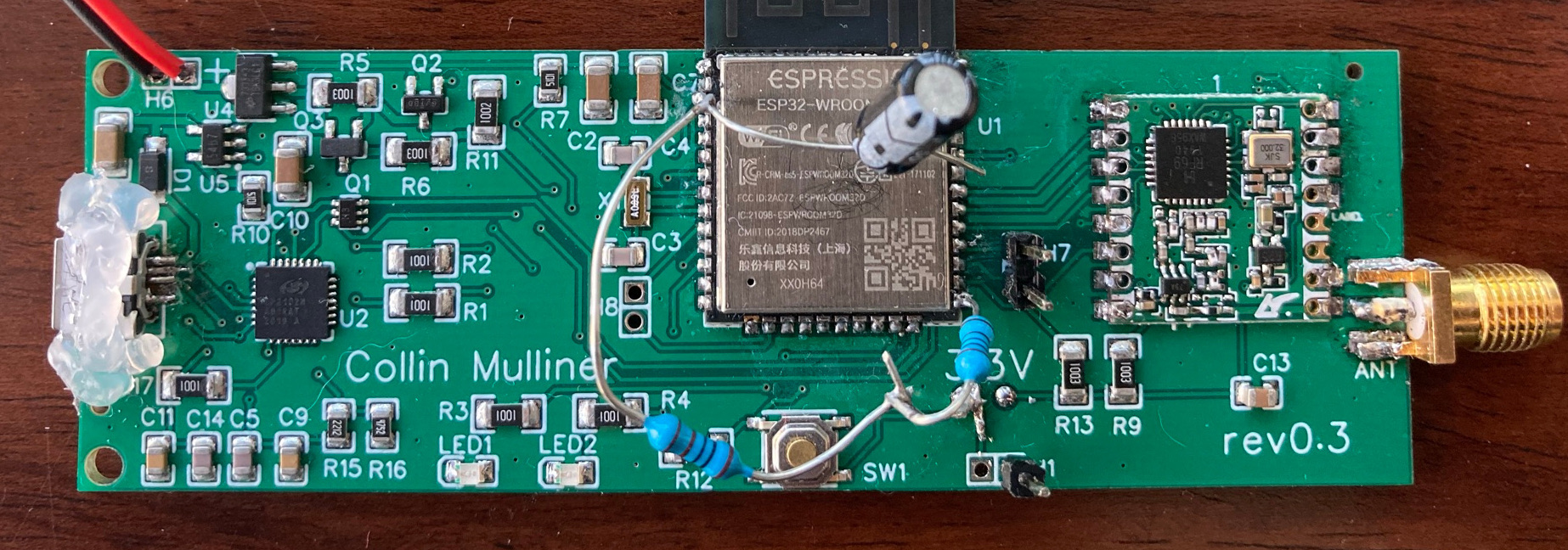
My first board was actually design number three (0.3). I ordered it in late September 2020. It arrived two weeks later. The board generally worked but had a number of issues. Below a picture of the board. I had to hand solder the micro USB port, the ESP32, the RFM95W, and the antenna connector. In this design I had through-holes for spare GPIOs, UART 2, and the spare 3.3V pin. You can see the unsoldered through-holes on the left of the ESP and the soldered UART 2 on the right side.


Let's talk about issues!

The main issue is very clearly visible in the picture. I forgot the pull-up resistors for the ESP32. This probably happened since I was hyper focused on all the other things that I just forgot to add the pull-ups. Without the pull-ups the ESP32 does not even start. *YAY*. Once I realized what I (didn't) do I added the pull-ups. Lucky me that I added the spare 3.3V pad in a location that is easy to reach. (Yes, there are lots of places to get 3.3V from but I was happy about the pad.) With that fix the board actually fully worked. Well Kinda. I also thought I had to add the capacitor, turns out that you don't (this was me still not fully understanding things).

The LDO was the next issue. I tried to get components with a low quiescent current. I picked a HT73xx LDO with only 4uA but turns out 250mA are not enough if you decide to use Wifi on the ESP32. This resulted in consistent brown outs.

Conclusions from the first board.

Overall this wasn't as bad as I thought it was gonna be. Yes, I spent many month to get to the point where I actually had a board with my name on it into my hands. The boards (I got 5 PCBs - the minimum oder quantity) actually worked after I added the pull-ups. I found out that not all of the boards could detect the external 32khz crystal. I determined this by writing a board test program. In the end I was extremely happy. I basically had designed some electronics and now I was holding it in my hands and it worked!

Second Board

Designing the second version (v0.4) was much easier since I most of the first board worked. I basically just added the missing pull-ups. Replaced the LDO with one that can deliver 500mA. Once that was done I looked into some more fun changes. I started with replacing one of the green LEDs with a red LED. I also added USB (power) detection via a voltage divider. I removed all through-hole connectors (but the battery connector) and replaced them with pads. At the end I also replaced most resistors and capacitors with smaller footprint versions (I went from 1206 to 0805). This allowed me to make the board a little smaller.

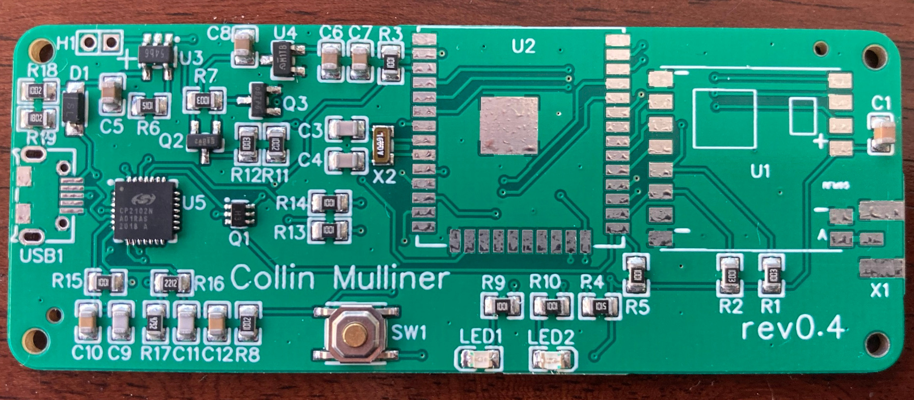
Below a picture of the v0.4 board as I received it from JLCPCB. You can see all of the components they soldered with just the USB connector, ESP32, RFM95, and antenna connector missing. JLCPCB just does not support those components in their prototyping SMT service.


Once I got all the components soldered the board worked as expected. I did most of the soldering for the v0.4 boards using reflow soldering with a hot air gun. I gained some experience with the hot air gun while soldering and re-working some of the v0.3 boards. I broke the very first v0.4 board because I didn't check the soldering on the USB connector. I had a short with the 5V and fried the USB serial IC. Four boards left.

Lets talk about the final design.

One of my original goals was to make a board that is capable of low power standby and sleep. The ESP32 has multiple sleep modes that help to decrease energy consumption and thus increase runtime on battery. Low power consumption is so much more besides the ESP sleep modes. From my understanding overall this requires a number of design choices. Things such as picking components with low quiescent current. Being able to completely turn off components that are not needed, e.g. the USB serial converter. In this design the USB serial IC is powered by USB VBus, this means if USB is not connected the IC is not active. It is not connected to the battery. This makes sense since you only need serial when connected to USB. At least for this specific board. The battery measurement circuit is another one that can lead to unwanted battery drainage. I found this battery measurement circuit as an example of how you can measure battery voltage without draining the battery too much.

For the RFM95W (LoRa modem) it is important to connect the DIO PINs as they are used as IRQs. Using IRQ instead of polling allows us to put the ESP into sleep and have the LoRa modem wake it up.

The schematic for Fluxboard v0.4 shows all of the circuits I mentioned. The 32khz crystal is required to if you want to use ESP32's dynamic power saving mode while using BLE.

Of course the second board is not flawless. The red and green LED are very different in their brightness. Apparently that is normal (I didn't know). I foolishly tried to design the board to always require a battery to be connected since VBus only inputs into the USB serial IC and the battery charging IC. In a new revision I would try to avoid that and be able to power the entire device via USB (in addition to a battery).

Conclusions

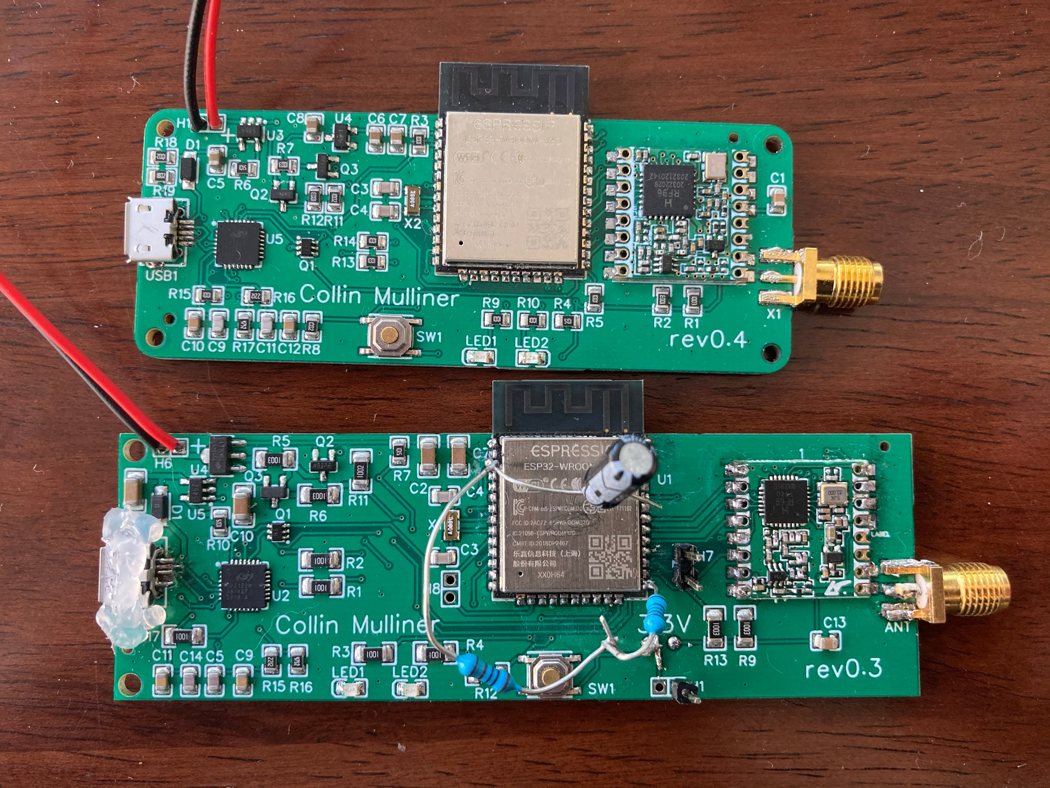
I really learned a lot going thru the exercise of design a board, making a revision, and having them produced. Working on the revision was much easier todo and much more fun. Below you can look at both board side by side, you can clearly see the progress from v0.3 - v0.4.


Also one thing to be very clear about. I basically ONLY learned how to make a custom ESP32 board. I don't think I could easily make something completely different without spending a similar amount of time on it. The progress of this projects was definitely driven by using a popular SoC that many people before me used for their own projects. To some degree it felt like software development that mainly uses stackoverflow answers to questions other people asked before you. Instead of software you build circuits. Like: how do I measure the battery voltage without draining the battery?

Many thanks to Idan Warsawski for giving me tips and directions for learning PCB design and providing feedback on my schematics.


comments:

your comment...

 
Name:
URL/Email: [http://... or mailto:you@wherever] (optional)
Title: (optional)
Comments:
Save my Name and URL/Email for next time (cookies required)